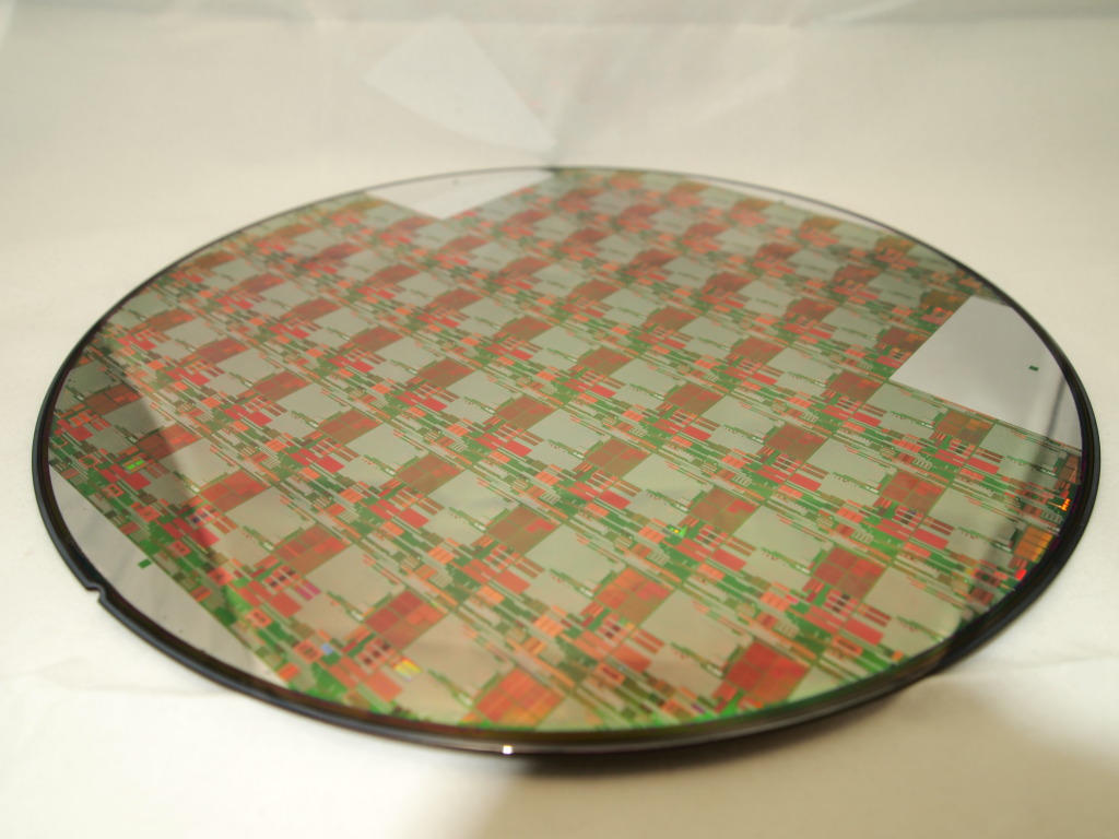
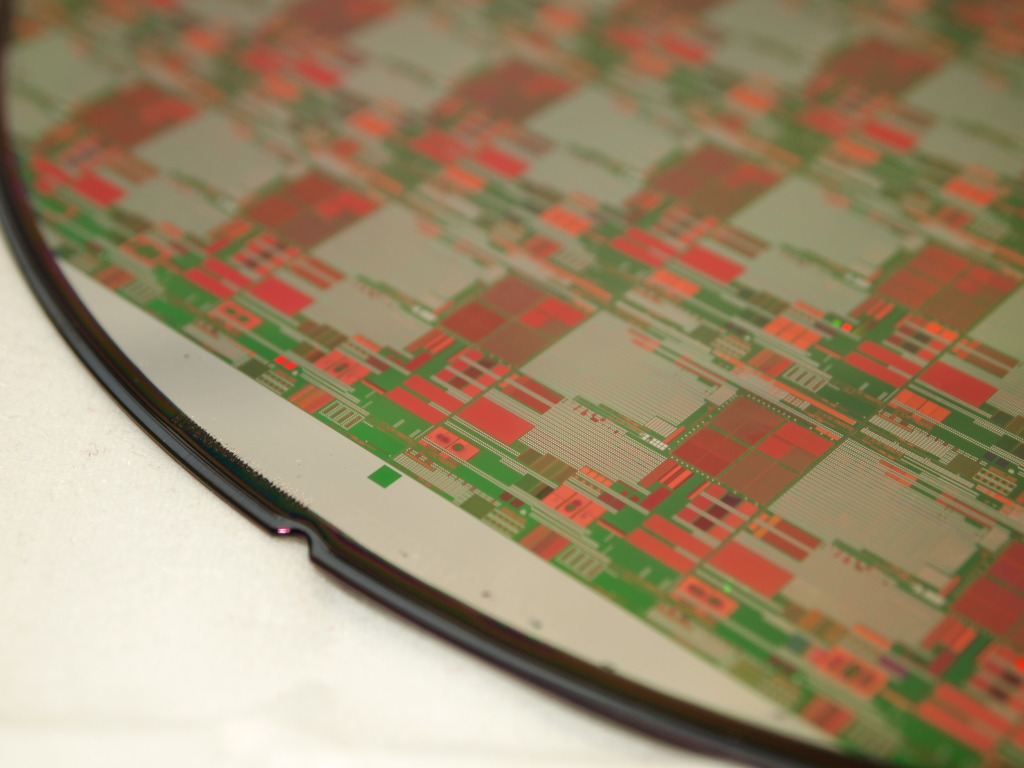
THESE WAFERS ARE TRULY A PART OF SEMICONDUCTOR HISTORY.
These wafers have etched circuits or test patterns that look absolutely fascinating under a microscope. Take a look at the low resolution shots I have here and imaging the wondrous detail you could see under a microscope instead of an iPhone camera!!
Each purchaser will get a single 8"/200mm wafer that is perfect in every detail - no cracks or chips. These wafers have some very very light surface visible surface scratches but are still great decorative objects - reflected in the great pricing
These wafers make a great talking point and are fascinating for engineers, students or indeed anyone interested in technology. The detail is amazing. Embedded in lucite or mounted in a nice frame with appropriate lighting these can and do look stunning and would make a nice addition to anyones den or study.
Great as an educational aid to show students how microelectronic circuits were made in the past and indeed are still made now - etched into pure silicon wafers, diced up and packaged.
At this price - what are you waiting for?


 Shopping Cart